Dies ist eine alte Version des Dokuments!
Inhaltsverzeichnis
Course A Power Electronics
Within this course, you will investigate the behavior of a buck converter through simulation and real measurements. Simulations will be carried out using LTSpice, which you can download at Analog Devices. For the measurements, you will receive our DIY power electronics evaluation board, equipped with three separately configurable half-bridges. The hardware is controlled using a Simulink experiment.
One main goal of the lab course is to train the usage of measurement tools such as oscilloscopes, current clamps, differential voltage probes, and more.
Simulation
The problem often arises that electronic assemblies such as microcontrollers, sensors, small actuators or motors have to be supplied with 5V from a higher-level voltage source, e.g. 20V.
Since linear regulators, which are nothing more than variable series resistors, generate excessive losses, buck converters are often used. With the use of modern semiconductors, efficiencies of > 98% can be achieved.
For our first experiment, we design a buck converter with the following properties:
Input voltage range: 15V … 24V, nominal 20V
Regulated output voltage: 5V
Rated output power: 25W
Ideal World
Unfortunately, a simulation is often very similar to installing real hardware: soldering everything together and applying voltage in the hope that it will work is utopian. Or in a simulation: parameterize all components, connect them and press the run button usually doesn't work 
This usually doesn't work even if we only use ideal components. We have to gradually start approaching the matter and build up the simulation step by step. And each step must confirm the results we expected at the beginning. If this is not the case, the simulation should be reduced or simplified again until the result meets our expectations in order to achieve a trustworthy result. Don't let a simulation lie to you.
It is just as important as the simulation itself to check whether the results are plausible. If, for example, currents > 100A or voltages in the MV range occur in the simulation, you should not trust the result under any circumstances.
Task 1a)
Create the circuit diagram of a buck converter consisting of a switching element, diode, coil, capacitor and load. Determine the load resistance so that the required power is set at the output.
Use LTSpice to create a simulation of a buck converter with the boundary conditions described above, consisting of an ideal switch, an ideal diode, coil and output capacitor.
Task 1b)
Create a table and sketch the voltage and current curves. Calculate the expected voltage and current values for each component at the nominal input voltage.
Task 1c)
Use LTSpice to create a simulation of a buck converter with the boundary conditions described above, consisting of an ideal switch, an ideal diode, coil and output capacitor.
Task 1d)
Compare the simulation result with the expected results. What do you notice? What explains the deviations?
Task 1e)
You may have noticed that although we asked LTSpice to use an ideal diode, it was not chosen as ideal. Use the simulation to calculate the efficiency of your buck converter.
For the simulation/calculation please use the following parameters:
Switching frequency: Last two digits of your Matrikelnummer in kHz ((if the value is less than 20, it is doubled until it is greater)
Inductor: Last three digits of your Matrikelnummer in µH (if the value is less than 40, it is doubled until it is greater)
Capacitor: Use a 330µF electrolyte capacitor.
Did you know? With LTSpice, it is very easy to calculate the RMS and average values for solutions in the time domain. Use Ctrl + left-click on the signal in the result view to see the calculated values.
Note: Within LTSpice you have to configure the switch parameters first:

Diodes always incur power loss, primarily caused by the voltage drop across the device. Thus, the freewheeling diode is often replaced by a second power switch, leading to the commonly used half-bridge topology. This is a clever solution, especially when using MOSFETs as switches. MOSFETs always come with an intrinsic diode, known as the body diode. Therefore, even if the MOSFET is not activated, the body diode can serve as the freewheeling diode. The body diode, of course, exhibits the same poor power loss characteristics as the previously used diode. Therefore, we activate the MOSFET to allow the current to flow through the MOSFET instead of the diode.The rule to avoid short circuits is as follows: whenever the high-side MOSFET is turned off, the low-side MOSFET is turned on. However, this introduces another problem. Since the switching speed of the devices is not infinite, a certain amount of delay is required before turning on the low-side MOSFET after the high-side MOSFET is turned off, and vice versa. This delay is referred to as dead time. With ideal switches, we do not need any deadtime. However, you can equip the PWM generator with a deadtime function, as we will need it later
Task 2a)
Replace the diode in your simulation with an additional ideal switch and run the simulation again. Now, the calculated current values should match the simulated ones pretty well.
Task 2a)
Once again, compare the simulation results with your expected values. Ensure that your simulation produces reasonable results, as values in the range of kA or MV are outside the expected scope!
Note: Dead time can be generated by shifting the comparator values with a negative or positive offset. In the following example, Qn is the inverse PWM signal of Q, with variable dead time.

Real Components
Adding Mosfets
LTSpice, like any network simulation program, is capable of accounting for the real behavior of MOSFETs. However, as we know, the parasitic elements of almost all semiconductors are strongly dependent on temperature. For MOSFETs, parasitics such as the parasitic capacitance are even dependent on the current voltage value.
Nevertheless, having a simple, realistic behavioral model is better than having none at all. The models can normally be downloaded from the manufacturer's website.
Here irf3205s.zip you can find the model for your IRF320 MOSFET.
Datasheet: irf320.pdf
Task 3a)
Replace the ideal switches with the MOSFET model. Be sure to set the correct gate-source voltages.
Task 3b)
Determine the required dead time for the MOSFETs to ensure safe operation. Observe and document what happens if the dead time is too short. Take a screenshot for your documentation.
Task 3c)
Adjust the duty cycle so that the output is set to 5V again.
To determine the required deadtime you can delete the load and increase the deadtime as long as there are short circuit pulses. Due to the parasitic mosfet capacities which are continuously charged and discharged, a remaining current can be seen even with sufficient dead time. In reality, however, this is not as large as in our almost ideal simulation environment, due to additional damping lead resistances or the internal resistance of the source.
Adding Gate Driver
In a simulation, it is very easy to generate an isolated voltage source that is independent of the common ground. In reality, generating isolated sources requires significant effort, as transformers are typically needed to decouple the grounding. The problem arises with the gate supply of the high-side MOSFET, as the drain potential continuously switches between the reference ground and the input voltage. A commonly used solution is the use of a so-called bootstrap circuit. Put simply, the circuit charges a capacitor which is then connected to the mosfet independently of the ground potential. Integrated circuits such as the IRS2890DS driver we use perform this task for us and can control one half-bridge at a time.
 Gate drivers are often equipped with additional features. Our driver can detect overcurrents and if necessary, will turn off all MOSFETs for safety. Since overcurrents in a simulation tool will not damage your PC or notebook, you can ignore this feature in the simulation. Pull up the RFE output and connect ITRIP to ground.
Datasheet: infineon-irs2890ds-ds-v01_00-en.pdf
Task 4a)
Add the driver circuit to your simulation and check the functionality. The general behavior should be the same as before! The simulation time now might significantly increases depending on how fast your computer is. Use the datasheed to complete the circuit.
Task 4b)
Now you can determine the switching time of the drive and the MOSFETs. Measure the required time to turn the MOSFETs on respectively off for every MOSFET.
Task 4c)
Since we cannot turn the switch off before it has fully turned on, a minimum on-time for the switch is required, which will define the maximum frequency. Calculate the maximum frequency we can use for this setup if we want to use a minimum duty cycle of 10%.
Check if the gate-source voltage of the MOSFETs can reach the full desired value to ensure the device turns on safely
As a rule of thumb, the bootstrap capacitor is selected in the range of the input capacitance Ciss of the MOSFET to be driven. However, many developers start with a 100nF capacitor and check the function in the design. During the turn on phase the voltage at the gate should be as constant as possible. What do you think?
Is a 100nF capacitor enough? Gate series resistors are used either to reduce the switching speed of the mosfets or to dampen unwanted oscillations. A value between 1 and 10 ohms is often used as the starting value.
Estimat Parasitics
Now we have a pretty good simulation of the buck converter to calculate the operation point and get a feeling for the losses. Simulation however ist getting slower and slower. To get even closer to the real behavior of ourbuck converter we have to consider the parasitic elements of the components.
- For the inductor we can add the series resistance given within the Datasheet: 74437429203101_100u.pdf
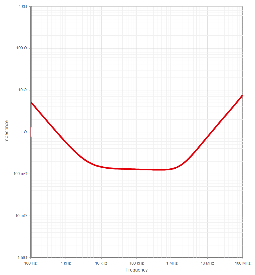
- The frequency behavior of the capcaitor can be calculated from the measured Z(f) plot z_f_330uf.png. Many manufacturers, such as Würth, offer the data for download on their homepage. Würth
- All PCB traces that carry a high current must be included in the overall consideration. The following values can be assumed as a rule of thumb. Inductance 1µH/m for supply lines or 10nH/cm for conductor tracks.The resistance can be estimated as 0,5mOhm/cm for a 35µm track with 1cm width.
Task 5a)
Add parasitic elements to the inductor, capacitor and pcb traces. Estimate a trace length to connect the MOSFET leads of about 1cm.
Task 5b)
Run the simulation again and describe the effect of the parasitic elements.
Task 5c)
Every trace and wire represents an inductor. Distinguish between good and bad parasitic inductors. Mark all critical inductors within a sketch or the schematic.
It might now be clear that the final output voltage does not depend solely on the duty cycle. In a real system, many parameters influence its behavior. This is one of the reasons why we need a control loop, which we will implement later in the lab.
Reactive Current
When we think of reactive currents or reactive power, we usually think of AC voltage systems but not of a step-down converter. But let's imagine the following scenario: The load resistor increases, or the load is lost— for example, because you turned it off or due to a broken connection. The DC-DC converter still attempts to regulate the output voltage to 5V with a constant duty cycle. In the half-bridge configuration, the high-side MOSFET will charge the output capacitor, while the low-side MOSFET discharges the capacitor within the same cycle. This creates a circulating current between the output capacitor and the power supply. You can easily demonstrate this behavior with a simulation. However, in the lab, it might be dangerous. Why? During the discharge of the capacitor, the circuit behaves like a boost converter. If the input voltage source cannot handle negative currents, it might get damaged. In many cases, however, the reactive current generates losses, and the bulk capacitor at the input of the buck converter can absorb the reverse current.
Task 6a)
Run the simulation with verly light load respectively a very high ohmic load resistor e.g. 100kOhms. Observe the capacitor current and the current through the MOSFETs. What is bad about this mode of operation?
Task 6b)
Find a solution how to prevent the drawbacks you have observed in task a) and run the simulation again. Please check the desired output voltage!
Task 6c)
How can you implement your solution within a microcontroller regulated buck converter?
DIY Power PCB
Hardware Introduction
For a quick introduction to the world of power electronics, we have developed the DIY Power Electronic PCB. It contains three half-bridges that can be controlled independently of each other. The PWM signals are generated by an ESP32 microcontroller whose frequency and duty cycle can be adjusted. The driver circuit and the mosfets correspond to the components you have already simulated.
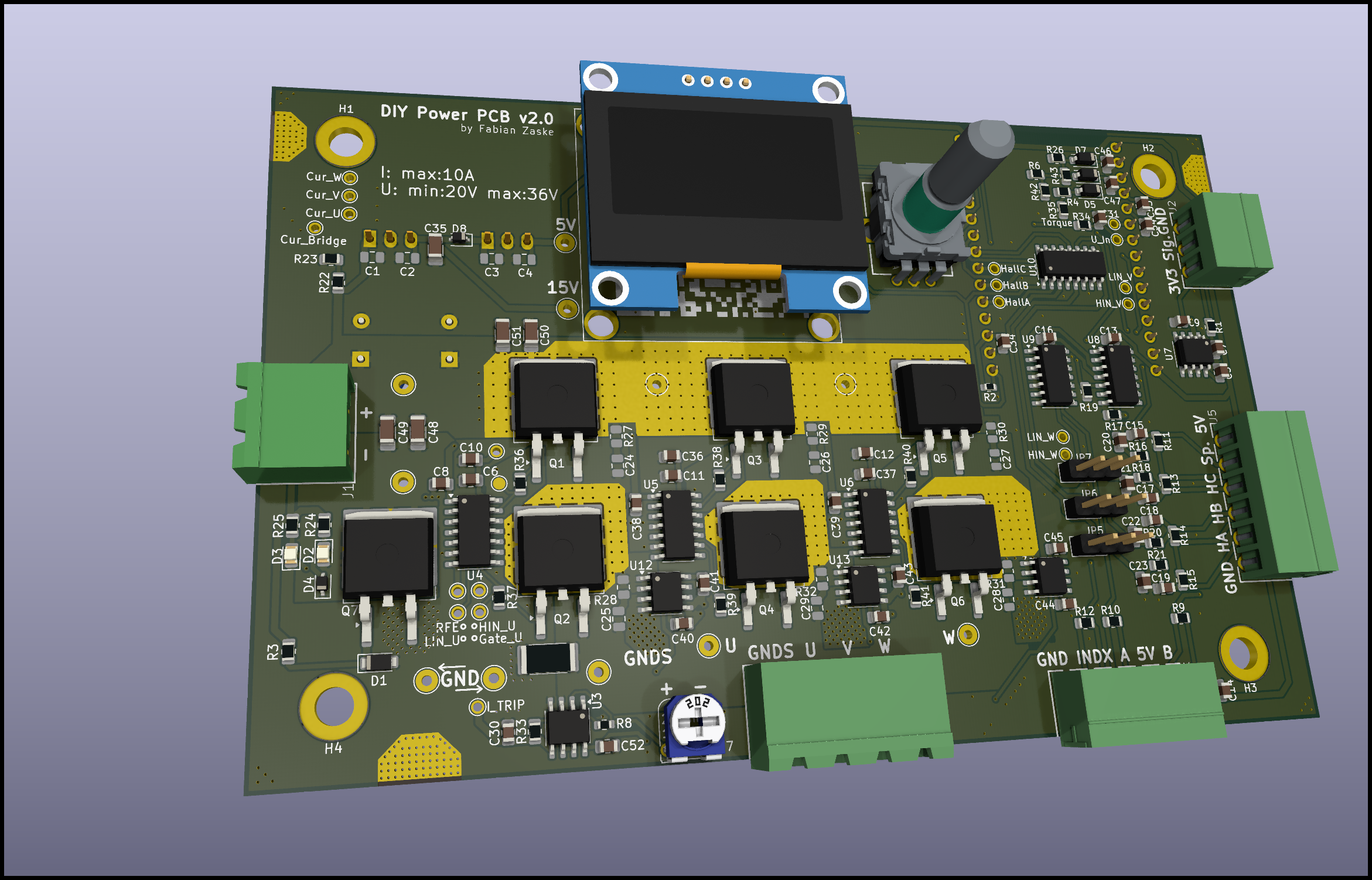
The PCB was originally not only developed for the power electronics lecture but also to drive different motor applications. Therefore, the PCB contains more features than are necessary for your measurements.
Download: schematic_diy_power_pcb.pdf
Task 7
Do you know the function of each component on the circuit board? If not, consider the function of the individual circuit parts together with the data sheet.
Inductor / Capacitor / Load
To investigate the behavior of the buck converter, we can connect different inductor and capacitor values. They can be individually connected using the connection cables.

You can choose between the following parts from Würth Electronic:
- Inductor: 74435584700
- Inductor: 74437429203101
- Capacitor: 860241081001
- Capacitor: 860010581025
Task 8
Complete the following tables using the data sheets. What do you notice in particular?
| Capacitor 1 | Capacitor 2 | |
|---|---|---|
| Rated Capacity [F] | ||
| Tolerance [%] | ||
| Max Voltage [U] | ||
| Max. Ripple [A] | ||
| Max Ripple at 5kHz [A] | ||
| Max Ripple at 10kHz [A] | ||
| Max Ripple at 20kHz [A] | ||
| Expected Lifetime [h] | ||
| Leakage Current [A] | ||
| Price, per piece [€] |
| Inductor 1 | Inductor 2 | |
|---|---|---|
| Rated Inductance [H] | ||
| Tolerance [%] | ||
| Max Voltage [V] | ||
| Saturation Current [A] | ||
| DC Resistance [Ohm] | ||
| Expected Lifetime [h] | ||
| Leakage Current [A] | ||
| Price, per piece [€] |
Please take a moment to answer the following questions for yourself:
- Compare the size of the capacitors in relation to the maximum allowed DC voltage and the capacitance.
- Wow, what a huge tolerance! Do you think every capacitor has such high tolerance values?
- Why is the maximum allowed ripple current a function of the frequency?
- What is the main parameter for the capacitor's lifetime?
Simulink
The power PCB is controlled with the help of a Simulink experiment. The microcontroller exchanges data cyclically with the PC via the serial interface.
- Connection, COM- Port, Start, Stop
Before you start
Although we designed our DIY power PCB hardware with many safety features, such as reverse polarity protection, fixed minimal deadtime, and overcurrent protection, it is, of course, still possible to easily destroy any power electronic circuit.
For every electronic circuit, there are two main golden rules:
- Voltage sources, especially capacitors, must not be short-circuited.
- Current flows must not be interrupted, especially if they are routed through inductors.
Especially the second rule is mandatory for power electronic circuits to avoid serious damage through overvoltages or electric arcs!
Safety warnings:
- The components and the load resistor can reach temperatures > 100°C, posing a risk of burns.
- If the polarity of the electrolytic capacitors is incorrect, they can explode or outgas. If you are not sure, please ask!
Therefore follow the procedure for each test setup:
- The power supply has to be switched off each time a change is made in the setup and during probe connections.
- Before you start a measurement, consider the points to be measured in the schematic. Use a printed copy of the schematic!
- Increase the Duty from zero to the final value.
- For safety reasons, please always deactivate the supply voltage when you leave your workplace.
PWM-Signals
The most important task of the microcontroller is to generate the PWM signals. Thus, we first start and check the signals.
Task 9a
Use two oscilloscope probes to visualize the output signals for the high-side and low-side MOSFET.
Task 9b
Measure the minimum and maximum of the adjustable deadtime.
Task 9c
Use the maximum deadtime and vary the frequency. Why is it not possible to use slow MOSFETs for high-frequency PWMs?
Task 9d
Set the frequency to 5kHz and set the deadtime to the value you have determined in task 3.
 MOSFETs with an SMD package such as D2Pack are commonly used. Even for measurements, they are suitable as we can directly connect to the pins. However, please be very careful when connecting the probes to avoid creating a short circuit. And very importantly: Turn off the power supply during any changes. A single short circuit can cause significant damage to the microcontroller or the driver IC.
Here you can find information about how to use differential voltage probes and our current clamp.
Starting conditions for the next measurement:
Frequency: 5kHz
Duty: 10%
Task 10a
Measure how long it takes for the driver to start doing anything when it receives a high signal and turns on the high-side MOSFET
Task 10b
How long does it take to bring the gate-source voltage to the desired value?
Task 10c
Determine the same values for turning the MOSFET off and for the low-side MOSFET.
Task 10d
Now set the frequency to 30 kHz. Does this make sense? What is your conclusion for the minimal duty cycle?
The result should look something like this:
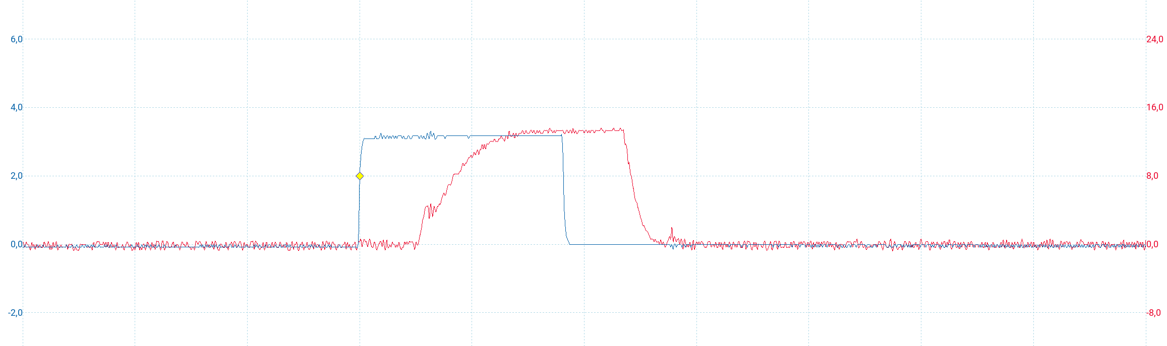
Take a screenshot of all four measurements for your report. Label the signals and the delay times. To work with stable signals on the oscilloscope, it is generally a good idea to use a PWM signal as the trigger source.
Half-Bridge Mode
Now is the time for us to let a current flow. In the first step, we measure the current flow with a purely resistive load, before we connect an additional inductance. In the last step, a capacitor smoothes the output voltage of our buck converter. Our first experiment is calculating the power consumtion of an ohmic load.
Starting conditions:
Frequency: 5kHz
Load resistor: 20Ohm
Duty: Ramp up to 50%
Task 11a
Connect the load resistor to the PCB so that the half-bridge U is loaded. Measure the output current using a current clamp. Does the measured current waveform match your expectations?
Task 11b
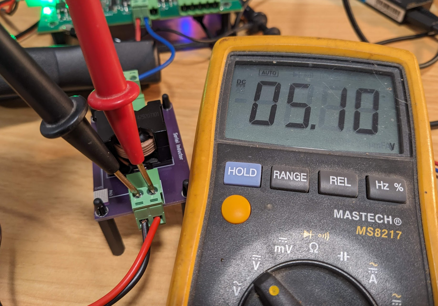
Measure the output voltage with a multimeter and compare the value with the voltage measured using the oscilloscope.
What type of measurement does the multimeter use?
Task 11c
Calculate the input power, output power, and efficiency. Check whether the values are reasonable.
Task 11c
Decrease and increase the duty and observe the current. Does this match our expectations?
At the latest, when we look at the voltage curve, it becomes clear that we can regulate the energy flow via the duty cycle but not the maximum output voltage. This means that even if we set the average value to 5V via the duty cycle for the power supply of a microcontroller, this type of voltage curve would certainly destroy it.
For this reason, we have to smooth the voltage curve. The first idea is to use a capacitor. However, due to the conservation of energy, the voltage on a capacitor must not jump. If we tried to do this, a very high current would flow into or out of the capacitor with every switching operation.
This leaves only a inductor that can be used as a storage element. So let's smooth out the voltage.
Starting conditions:
Frequency: 5kHz
Load resistor: 20Ohm
Inductor: 47µH
Duty: Ramp up to 50%
Task 12 Set the starting conditions and observe the inductor current.
If we ramp up the duty cycle to the target value, you may already be able to hear it. The inductance oscillates with the clock frequency, which can produce a rather unpleasant beeping noise.
Task 13a
To get rid of the noise increase the frequency to 20kHz and observe the current again.
Task 13b
Now use the 100µH inductor and try again. Obeserve the inductor current. What is your conclusion? (Look at the current ripple with the scope)
If your are not sure, measure output voltage with the oscilloscope and the differential probe.
Now lets increase the current. Take the 3,3Ohm slide resistor and set it to 1Ω (check with the multimeter!)
Reminder: Turn all Mosfets off and set the duty to 0% before you make any changes at the setup!
Task 13c
Increase carefully the duty cycle until we reach the desired value of 5V/5A, 25W.
Task 13d Measure the voltage across the inductor and the output.
Okay, it's still not ideal. If you want, you can increase the inductance value, adjust the frequency (max. 40 kHz), and observe whether you can further reduce the ripple current.
It is not possible to use a capacitor directly at the bridge output, but can of course use a capacitor after the inductor. Let's try this out.
To smooth the output voltage, we need capacitance values in the mF range. Only electrolytic capacitors are suitable for this purpose. These are very sensitive to polarity reversal. If this happens, the lab will probably be over for all participants that day
 First use a multimeter to check whether the designations on the circuit board match the measured polarity before connecting the capacitor. It might be possible that the incuctor is in the return current path by mistake.
In the next task, we will try to smooth the output voltage and reduce the output current ripple using capacitors. For a higher resolution of the ripple, you can filter out the average value of a signal by switching to AC coupling on the oscilloscope. As a result, a capacitor is connected in series with the signal at the oscilloscope input, blocking the average value. It is now possible to fully zoom out the remaining ripple and determine it using the cursor.
Task 14a
Set the duty cycle so that 5V is present at the output. Add different capacitor values and observe the remaining voltage ripple at the output.
Task 14b
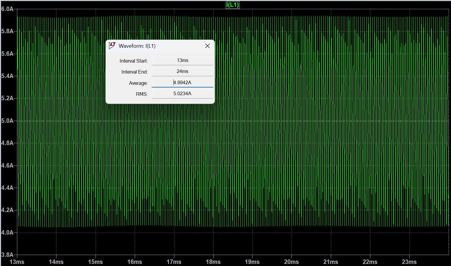
Now use the 4700µF capacitor and determine the inductor current (ripple, RMS and average value) and output
voltage ripple.
Task 14c
Do you have any idea what the current through the capacitor looks like? Create a sketch.
Hot surface! Please check the temperature of the components (coil, circuit board, mosfets, capacitor, ….) from time to time. You can use an infrared thermometer for this purpose.
Please be careful when checking the temperature with your finger 
Measurement, Simulations and Calculations
Your buck converter is almost ready. Now it is a good time to compare the measurement results with the simulation and calculations.
Please use the following parameters:
Switching Frequency: 20kHz
Inductor: 100µF
Capacitor: 4700µF
Load: 25W, 5V, 5A
Input voltage: 20V
Task 15a
Calculate and simulate the behavior of the converter with the given values. Compare those values with the ones you measured.
Is there any deviation? If so, explain its possible causes.
Task 15b
Update your simulation that takes the real components into account and check whether the results are better.
Task 15c
Try to match the simulation with the real measurements.
Task 15d
Determine the losses of all components and calculate the efficiency in simulation and measurement.
Task 15e
Measure the temperature of all critical components and display the values in a list. How can you find out whether you have reached the thermally steady state?
Task 15e
Estimate the Rth value for the PCB mounting of the MOSFETs using the measured temperature value.
Reactive Current
Voltage ripple due to the remaining current ripple might not be a problem, as we can cancel the voltage ripple with capacitors. But there is a big problem:
Consider your DC/DC converter has nothing to do because the load is turned off — for example, any device that is in standby or low energy consumption mode. The output voltage is still set by the duty cycle to 5V. If you look at your formula to calculate the current ripple, nothing really changes. Thus, the current ripple through the inductor is still the same as calculated before. Even if we turn off the load, the remaining current ripple is heating up our components.
Task 16a
Disconnect the load and set the output voltage to 5V. Measure the inductor and capacitor current.
Task 16b
Calculate the no load efficiency of your buck converter.
Continuous / Discontinuous and Critical Current Mode
The transition from the point at which current flows back out of the capacitor occurs from the so-called critical current mode. Here, the lower reversal point of the current is set on the zero line. If the load becomes even smaller, the current in the capacitor becomes negative and flows back to the source as reactive current.
Task 16a
alculate the critical load resistance at which critical conduction mode (CRM) occurs.
Task 16b
Increase the load resistance until you can measure the CRM state. Check what happens if you increase the resistance further.
Reactive currents are not always bad. They can be used to eliminate the reverse recovery of the body diode. If we exactly meet the CRM mode, there is even no switching loss because we turn on the low-side MOSFET at zero current. If it is possible to generate a small amount of negative current, we even have no switching losses at the high-side MOSFET, as it operates in zero-voltage switching. This type of power electronic circuit is called a resonant converter, and it is now commonly used in many applications. The theory behind resonant switching converters is part of the Master's course Power Electronic Systems.„
The reduction of the reverse recovery effect can be seen by measuring the current through the MOSFETs with a Rogowski coil. If you don't have one, it is also possible to look at the drain-source voltage of the low-side MOSFET.
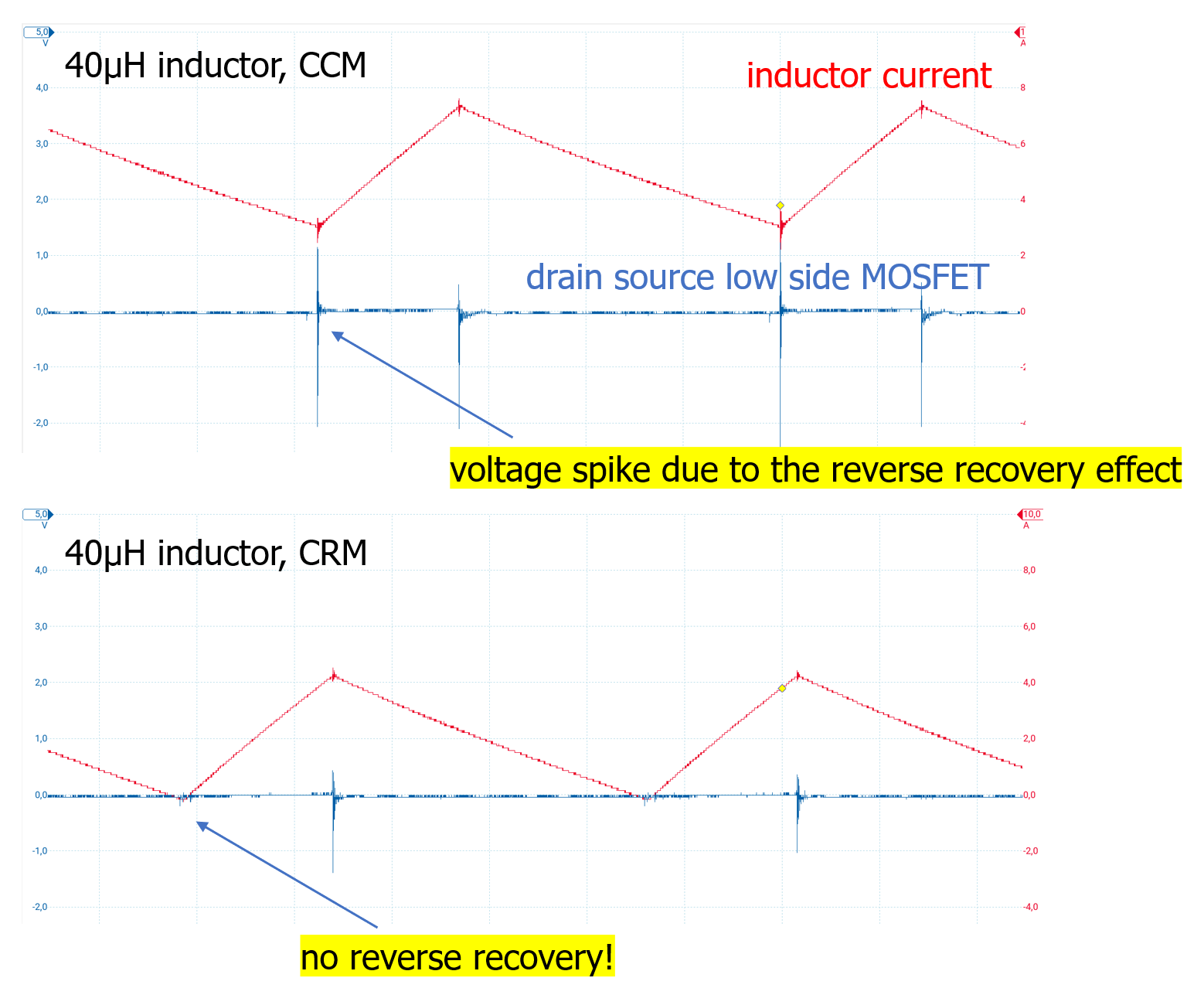
Task 17a
Consider and discuss with your neighbor why in this state the high side mosfet can be switched on at a voltage of less than 1V. This state is then referred to as ZVS zero voltage switching.
Congratulations. Now you are ready and prepared for the exam!